

Understanding
power supply noise.
|
||
|
Linear supplies versus switching supplies
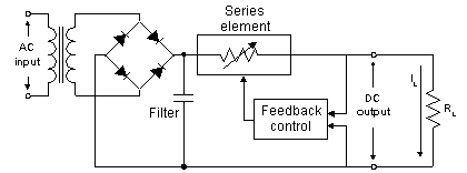
Power supplies come in two basic flavors: linear and switching. Linear designs are the easiest to understand. The level of the rectified dc signal is controlled by a series-pass transistor that operates like a variable resistance. When you adjust the output level on a linear supply, you're essentially adjusting the bias voltage of this transistor. This straightforward approach provides low output noise and fast programming response, but it suffers from lower efficiency and a high ratio of size and weight to output power, thanks to the large power transformer.
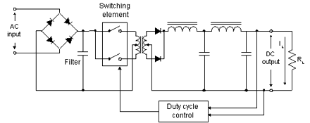
In a switching power supply (sometimes called a switched-mode supply or simply a switcher), the output level is controlled by an switching element such as an FET H-bridge working in tandem with a pulse width modulator. When you adjust the output level, you're controlling the pulse width from this modulator. The width of the pulse determines the duty cycle of the FET bridge, thereby adjusting the power passed to the transformer and on to the output filter. The switching architecture is more efficient and can deliver more power in a smaller package (the HP 66000 modular power supply offers eight individual supplies in only seven inches of rack space, for instance). The downside, as you probably guessed, is the noise generated by all the switching activity. The good news is that recent advances in switcher designs have dramatically reduced noise levels. Knowing what kind of supply you have (all the supplies in the HP Basic Instruments family are linear designs) is a key step in understanding the type of noise it's likely to generate, as you'll see in the following sections on normal and common mode noise. Normal mode noise Normal mode noise generated by a supply shows up as an undesirable voltage at the output of the supply, in series with the output voltage. It contains both periodic and random components. In fact, it's often called PARD, for periodic and random variations. You'll see it listed in HP data sheets as ripple and noise (the periodic and random components, respectively). The HP E3633A supply, for instance, has specified performance of <350 µVrms/2 mVp-p and <2 mArms. The nature of normal mode noise The nature of ripple depends on the power supplies. In linear supplies, it's usually related to the ac power frequency (usually at twice the frequency as a result of full-wave rectification). For 60 Hz power, for example, ripple shows up as a 120 Hz signal. In switching power supplies, ripple is a function of the switching frequency and is usually in the range of 20 to 100 kHz. Noise encompasses random signals from a wide variety of sources, including messy ac power, noisy regulator parts and rectifier diodes, and coupling from adjacent digital circuits. Because it doesn't stem from a single source, random noise presents a complicated engineering challenge in which every potential source must be considered. Minimizing noise calls for careful design and top-quality components throughout. How normal mode noise affects your circuits
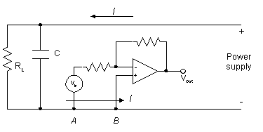
To get an idea of how power supply noise can affect a circuit, consider a basic operational amplifier. Typical op amps have a power supply rejection ratio (PSRR) of 75 dB for low-frequency ripple. If the power supply contains, say, 0.5 mVrms of ripple, the op amp will refer about 90 nVrms of that to the output. Random noise, however, has higher frequency content, and the PSRR rolls off at 20 dB per decade. In other words, much of the random content will be transferred directly to the op amp's output, and the higher the frequency content, the more output noise. Ground currents present another opportunity for supply noise to play games with your circuit. In the accompanying circuit diagram, the ground current I, which could be from the amplifier load or a bypass capacitor, contain the power supply noise. If I is equal to 100 mA and there is 1 mV of noise on a 12 V supply, the result will be noise current of at least 8.33 µA (depending on the frequency content of the noise in the case of capacitive reactance). The resistance of the circuit trace between points A and B in the diagram creates a voltage drop, and this voltage is in series with the input signal. If you have a java enabled browser try our noise calculator application of the table below.
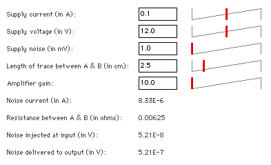
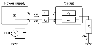
To see what effect this noise could have on the op amp's output signal, start by entering the supply current in amps and the supply voltage in volts, then the supply noise, which is in mV. Next, enter the length of the circuit trace between points A and B in centimeters (the calculator assumes trace resistance of 0.01 ohms/cm, a fairly typical value). Then enter the gain of the op amp to see the effect on the output signal. The calculator will then show you the noise current I, the resistance between points A and B, the noise voltage across A and B (which is fed directly into the op amp), and the resulting noise added to the output signal. It shouldn't take much to demonstrate the importance of low power supply noise when you're dealing with sensitive signal levels. Common mode noise In its simplest form, common mode current (CMI) noise is a current that flows between the output terminals of the supply and earth ground. CMI noise can cause unexpected problems when it is transformed into a noise voltage by imbalances in the common mode impedances of the circuit or device under test and by any imbalances in the leads from the power supply. The result can be higher noise levels than the supply nominally generates. When you're testing in a situation like this, a circuit or device that actually has acceptable noise tolerance levels can appear to fail because it's really receiving more noise at the inputs than you think it is. The nature of common mode noise With linear supplies, CMI noise appears as a distorted sine wave related to the ac supply voltage and is usually not a problem as long as one terminal is grounded. CMI noise in a good linear supply is typically less than a microamp. With switching supplies, particularly older models, CMI can be a problem even when one terminal is grounded. CMI noise appears as high-frequency pulses, and traditional designs produced enough CMI to lock switching supplies out of noise-sensitive applications. How common mode noise affects your circuits
The accompanying circuit diagram shows a simplified model of CMI with a power supply connected to a circuit under test. The load is represented by two impedances, Z3 and Z4. Both are connected to earth ground through Z5, which can be a short, a resistance or a capacitance. The CMI flows from both power supply terminals to this earth ground. It creates a voltage along that path, which is of course equal to the CMI times the path impedance. For linear supplies, the CMI is at 50 or 60 Hz, and you have few worries about capacitance or inductance through the circuit. With the higher frequency CMI in switching supplies, however, capacitance and inductance can present major impedances, leading to significant noise voltage drops. (Some of the moves you can make to minimize this problem include making Z5 very high, balancing Z3 and Z4 to cancel common mode signals, and moving Z5 to the circuit inputs at points C or D. Of course, you don't always have these options.) The leads from the power supply to the circuit under test are also potential troublemakers. If the two leads don't have identical impedances, the differential voltage drops will show up as common mode noise at the inputs of the circuit under test. As mentioned above, though, recent breakthroughs in switcher design have greatly reduced the CMI problem. Whatever supply you use, take a minute to review its noise specifications and the impact its noise could be having on your circuits.
|
||